Beijing Haina Lean Technology Co., Ltd is one of the most
professional PCB manufacturer in Beijing,China. With more then 10
years of development, Haina Lean Electronics turns into a first
class manufacture of HDI PCB ,with production capability 4000
square meters.
Our factory is providing high quality bare PCB, PCB layout design
service and PCB assembly service,including components sourcing,
function test,conformal coating and complete assembly for clients
all.
We have profuse experience in manufacturing PCB,owned experienced
technical R & D technology team, young and professional sales and
customer service team, experienced and professional procurement
team and assembly testing team, which make sure the products
quality of the pass rate, on-time delivery rate of customer orders.
Our services include: circuit board design and layout, 2-46 layers
PCB manufacturing, professional FPC production, electronic
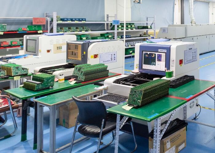
components purchasing, SMT professional processing, Soldering and
Assembly, especially sample and small bulk orders. we have the
advantages of a quick quote, fast production, fast delivery.
Beijing Haina Lean Technology is a one-stop EMS supplier
integrating PCB design, PCB manufacturing, Component sourcing and
PCB assembly.
The company is specialized in electronic products supporting
processing services, mainly to undertake circuit board design,
layout production, components procurement, PCB plate making,
circuit board welding assembly debugging and other OEM/ODM
services.
Our first factory is located in Changping District, Beijing, the
main radiation Haidian, Changping, Chaoyang three areas of Beijing.
Since our company’s establishment, we have been adhering to
creating high quality, high efficiency, low-cost business
philosophy based on the circuit board processing industry for
customers. Most of the key staff of the company are mature
technical talents who have been engaged in the industry for more
than 10 years, and have rich experience in the production of SMT
and DIP, also has rich experience in production for high density &
difficulty to package components such as BGA. We obtain a good
reputation in the industry through the continuous efforts of all
staff and high quality service . Our second branch plant is located
in Langfang city, and mainly cover Fengtai and Daxing Yizhuang
area.
The company pursues "inclusiveness, excellence, people-oriented".
Constantly innovate, take technology as the core, regard quality as
life, and wholeheartedly provide customers with high-quality and
high-efficiency humanized services.We are willing to serve our
customers with the principle of continuous honesty &
trustworthiness, pragmatism and innovation.
At present, the main cooperation industries are automotive
electronics, communications, audio and video, optoelectronics,
robotics, hydroelectric power, medical care, aerospace, education,
radio frequency, power supply etc industries.