FR 4 Multilayer (5+2+5) High-Density Interconnect HDI PCB Board
Manufacturing
HDI PCB Board Introduction
Haina lean Electronics is a one-stop EMS supplier integrating PCB
design, PCB manufacturing, Component sourcing and PCB assembly.
The company is specialized in electronic products supporting
processing services, mainly to undertake circuit board design,
layout production, components procurement, PCB plate making,
circuit board welding assembly debugging and other OEM/ODM
services.
HDI PCB Board Manufacturing also known as high-density interconnect
PCB, is a kind of PCB with a higher wiring density per unit area
than traditional boards. HDI boards are more compact and have
smaller vias, pads, copper traces and spaces. As a result, HDIs
have denser wiring resulting in lighter weight, more compact, lower
layer count PCBs. HDI PCB is more fit into the little spaces and
have a smaller amount of mass than conservative PCB designs.
Factory Capabilities
| Item | Capabilities |
| Number of Layers | 1 - 36layers |
| Order Quantity | 1pc - 10000+pcs |
| Material | FR4 standard Tg 140°C,FR4 High Tg 170°C, FR4 and Rogers combined
lamination |
| Board Size | 700*610mm |
| Board Thickness | 0.3mm - 3.5mm |
| Copper Weight (Finished) | 0.33oz - 6.0oz |
| Min Tracing/Spacing | 3mil |
| Solder Mask Sides | As per the file |
| Solder Mask Color | Green, White, Blue, Black, Red, Yellow |
| Silkscreen Sides | As per the file |
| Silkscreen Color | White, Black, Yellow ,Etc |
| Surface Finish | HASL - Hot Air Solder Leveling |
| Lead Free HASL - RoHS |
| ENIG - Electroless Nickle/Immersion Gold - RoHS |
| Immersion Silver - RoHS |
| Immersion Tin - RoHS |
| OSP - Organic Solderability Preservatives - RoHS |
| Min Annular Ring | 4mil, 3mil - laser drill |
| Min Drilling Hole Diameter | 6mil, 4mil - laser drill |
| HDI Capabilities | HDI ELIC (5+2+5) |
| Other Techniques | Flex-rigid combination |
| Via In Pad |
| Buried Capacitor (only for Prototype PCB total area ≤1m²) |
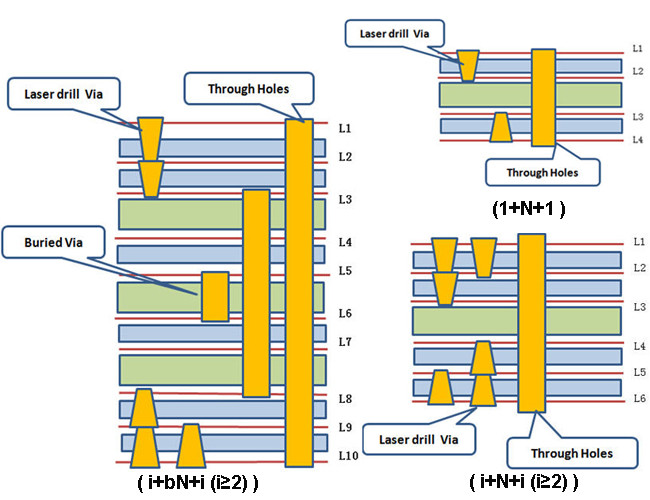
The types of HDI PCB
1.through vias from surface to surface,
2.with buried vias and through vias,
3.two or more HDI layer with through vias,
4.passive substrate with no electrical connection,
5.coreless construction using layer pairs
6.alternate constructions of coreless constructions using layer
pairs.
Work flow for HDI
Board Cut - Inner Wet film -DES - AOI - Brown Oxido - Outer Layer
Press - Out Layer Lamination - X-RAY & Rounting - Copper reduce &
brown oxide - Laser Drilling - Drilling - Desmear PTH - Panel
plating - Outer Layer dry film - Etching - AOI- Impedance Testing -
S/M Pluged hole - Solder Mask - Component Mark - Impedance testing
- Immersion Gold -V-cut - Routing - Electrical Test - FQC - FQA
-Package -Shipment

Our Service
1.PCB design:
we can provide circuit design & PCB layout support. | 5.Component procurement:
we have rich experience purchasing & material control expertise
team. |
2.SMT Assembly:
Leading edge surface mount population technologies. | 6.Complete turnkey solutions |
3.PTH Assembly:
RoHS compliant wave soldering & hand soldering capabilities. | 7.Function Test & Inspection: |
4.PCB Fabrication:
You only need provide Gerber files or other design files . | 8.We offer test & inspection services on PCB & Assembly
(X-ray,ICT, AOI and Functional tests) |

WorkShop


Advantages of HDI PCB
1.High Component Density
2.Space-saving
3.Lightweight Boards
4.Fast Processing
5.Save Number of Layers
6.Accommodate Low Pitch Packages
7.High Reliability
HDI PCB Application Field
HDI PCB board are mainly used for many industries , Like :
Automotive ; aerospace industries;medical devices;Industrial
automation,etc .
Except mentioned above, you'll also can find high-density
interconnect PCBs in all types of digital devices, like smartphones
and tablets, in automobiles, aircraft , mobile /cellular phones,
touch-screen devices, laptop computers, digital cameras, 4/5G
network communications, and military applications such as avionics
and smart munitions.
Delivery Time
| Product Type | Qty | Normal lead time | Quick-turn lead time |
| SMT+DIP | 1-50 | 1WD-2WD | 8H |
| SMT+DIP | 51-200 | 2WD-3WD | 1.5WD |
| SMT+DIP | 201-2000 | 3WD-4WD | 2WD |
| SMT+DIP | ≥2001 | 4WD-5WD | 3WD |
| PCBA(2-4Layer) | 1-50 | 2.5WD-3.5WD | 1WD |
| PCBA(2-4Layer) | 51-2000 | 5WD-6WD | 2.5WD |
| PCBA(2-4Layer) | ≥2001 | ≥7WD | 5WD |
| PCBA(6-10Layer) | 1-50 | 3WD-4WD | 2.5WD |
| PCBA(6-10Layer) | 51-2000 | 7WD-8WD | 6WD |
| PCBA(10-HDILayer) | 1-50 | 7WD-9WD | 5WD |
| PCBA(10-HDILayer) | 51-2000 | 9WD-11WD | 7WD |
Partners

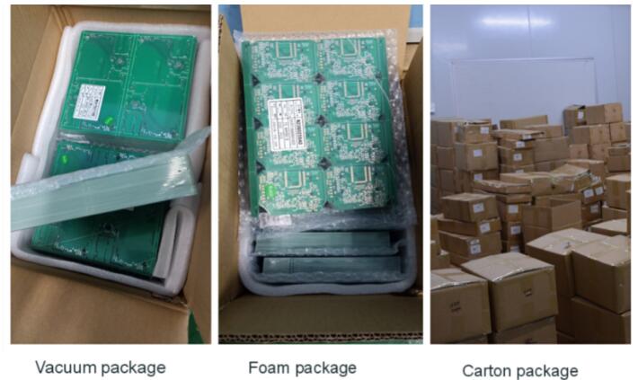
Common packaging
PCB: Vacuum packaging with carton box
PCBA: ESD packaging with carton box
Company Information
Beijing Haina lean Electronics Co.,Ltd is one of the most
professional PCB manufacture in Beijing,China. With more then 10
years of development, Haina Lean Electronics turns into a first
class manufacture of HDI PCB ,with production capability 4000
square meters.
Our factory is providing high quality bare PCB, PCB layout design
service and PCB assembly service,including components sourcing,
function test,conformal coating and complete assembly for clients
all.
We have profuse experience in manufacturing PCB,owned experienced
technical R & D technology team, young and professional sales and
customer service team, experienced and professional procurement
team and assembly testing team, which make sure the products
quality of the pass rate, on-time delivery rate of customer orders.
Our services include: circuit board design and layout, 2-46 layers
PCB manufacturing, professional FPC production, electronic
components purchasing, SMT professional processing, Soldering and
Assembly, especially sample and small bulk orders. we have the
advantages of a quick quote, fast production, fast delivery.
The company pursues "inclusiveness, excellence, people-oriented".
Constantly innovate, take technology as the core, regard quality as
life, and wholeheartedly provide customers with high-quality and
high-efficiency humanized services.We are willing to serve our
customers with the principle of continuous honesty &
trustworthiness, pragmatism and innovation.


